
Tata Electronics Signs 16 MoUs at SEMICON India 2026, Boosting Dholera Semiconductor Ecosystem
Tata Electronics signed 16 MoUs at SEMICON India 2026 with Indian and global partners, covering semiconductor manufacturing, materials, packaging, equipment and talent development linked to its Dholera and Assam facilities.
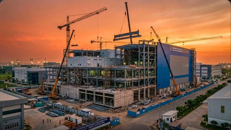
Tata Electronics signed 16 Memorandums of Understanding (MoUs) with domestic and international companies and institutions during SEMICON India 2026, held in New Delhi from September 17 to 19. The agreements are aimed at strengthening India’s semiconductor supply chain and developing supporting capabilities around Tata Electronics’ semiconductor projects in Dholera, Gujarat, and Jagiroad, Assam.
The partnerships cover several parts of the semiconductor value chain, including manufacturing, semiconductor materials, advanced packaging, equipment, infrastructure, supply-chain localisation and workforce development. The agreements involve partners from countries and regions including Japan, Europe, Malaysia and Singapore, along with Indian companies and institutions.
For Dholera, the agreements are particularly relevant to the development of the semiconductor fabrication ecosystem. Tata Electronics is developing a semiconductor fabrication facility in Dholera in partnership with Powerchip Semiconductor Manufacturing Corporation (PSMC) of Taiwan. The company has said that the facility is progressing according to the planned schedule.
Among the partnerships announced at SEMICON India 2026, Tata Electronics signed agreements covering semiconductor materials and manufacturing support for the Dholera facility. The company announced a partnership with Fujifilm to support localisation of critical semiconductor materials in India. Another agreement with JSR covers the supply of photoresists and advanced chemicals for the Dholera fab. Tata Electronics also partnered with Sumitomo Chemical for semiconductor materials and with Sojitz Corporation and NRS Corporation to develop the materials supply chain for the Dholera facility.
Tata Electronics also entered into a partnership with Kelington, a Malaysia-based engineering solutions company, to support critical infrastructure and systems required for semiconductor manufacturing at the Dholera fab. According to Tata Electronics, the collaboration is intended to support the facility’s operational readiness for silicon wafer production and also explore local talent development and engineering capabilities.
Another important agreement was signed with Ascendas First Space for the development of a proposed 363-acre vendor park in Dholera. The proposed park is intended to support the supplier ecosystem around the semiconductor fabrication facility. The agreement is part of the broader effort to establish supporting infrastructure and suppliers closer to the semiconductor manufacturing site.
The agreements also extend beyond Dholera. Tata Electronics signed a partnership with Nexperia covering semiconductor wafer manufacturing, assembly and testing, technology collaboration and innovation. The company also partnered with BESI Singapore to develop advanced semiconductor packaging capabilities in India. An agreement with the Semi-Conductor Laboratory focuses on semiconductor design services, process technology, supply-chain localisation and talent development.
Workforce development is another part of the wider semiconductor ecosystem being developed by Tata Electronics. The company partnered with Gati Shakti Vishwavidyalaya, along with L&T EduTech and Jacobs Solutions, to support talent development in semiconductor facility engineering and infrastructure systems. Tata Electronics has also said that Indian graduates are undergoing technical training at PSMC’s fabrication facilities in Taiwan as part of workforce preparation.
The 16 MoUs announced at SEMICON India 2026 reflect Tata Electronics’ effort to build a broader network of suppliers, technology partners, engineering companies and institutions around its semiconductor operations. For Dholera, the partnerships cover areas ranging from materials and engineering infrastructure to vendor development and operational readiness.
The development also comes as India expands its semiconductor ecosystem under the Semicon 2.0 programme, with the government focusing on semiconductor design, manufacturing, equipment, advanced packaging, research and development, and talent development. The Dholera facility is therefore part of a wider effort to establish semiconductor manufacturing and supporting industries in India.